TUTORIAL - PART 3
13) What determines the temperature limits of a semiconductor device?
The operating temperature limits (low and high) of a semiconductor device are determined by a number of factors, including
- The properties of the basic semiconductor material (Si, GaAs, SiC, ...).
- The type of device (diode, bipolar transistor, field-effect transistor, ...).
- The design of the device (materials, geometry and dimensions).
- The materials and designs of the contacts and interconnections.
- The assembly and packaging techniques and materials.
- The type of circuit in which the device is used (analog or digital) and the circuit design.
- What is meant by "operating temperature limit" and the particular application.
- How long the device needs to operate at the extreme temperature.
Let's consider these factors in turn, for both the low-temperature and high-temperature limits. Since there are so many combinations and interplay of the above factors, there are no simple and universal rules about temperature limits. Thus the following should be regarded only as a brief introduction.
As temperature is extended above or below the "conventional" limits (−55/−65°C to +125°C), the characteristics of a semiconductor device will continue the familiar trends that they exhibit within the "conventional" temperature range. However, at some temperature, other factors can come into play that cause unpredictable changes in characteristics—extrapolation is undependable.
14) What are the temperature limits of the basic semiconductor materials, and why?
Semiconductor devices operate by means of the movement of charge carriers (electrons and holes). The key is controlling their movement through arrangement of n-type, p-type, and intrinsic regions (and insulators) that have different electrical properties. A simple example is the p-n junction, which—as a result of different doping on the two sides of the junction—favors carrier movement in one direction across the junction but not in the opposite direction.
However, at sufficiently high temperatures the electrical difference between the n and p regions disappears and the p-n junction becomes ineffective in controlling carrier movement. This comes about as follows: as the temperature increases, the increased thermal energy ionizes significant numbers of the semiconductor atoms themselves (for example the Si atoms) in addition to the dopant atoms. This contributes additional electrons and holes in the conduction and valence and bands and, more important, results in approximately equal numbers of carriers in each band, independent of the doping, resulting in a condition called intrinsic. Since there are orders of magnitude more semiconductor atoms than dopant atoms, the influence of the dopant is overwhelmed at a sufficiently high temperature. The result is that the p-n junction becomes merely a fancy resistor that no longer controls the carrier flow, and leakage currents in devices can become so large that operation is disrupted.
Thus, in principle the basic upper temperature limit of each semiconductor material is determined by its bandgap energy. A rule-of-thumb is that the maximum temperature (in K) is approximately 500 times the bandgap energy in eV. For Si this rule gives Tmax ~ 500 x 1.12 ~ 560 K ~ 290°C. (Actually Si devices have been operated to about 500°C as mentioned earlier in Tutorial #1.) However, there may be other limiting effects, such as decomposition of the semiconductor material, that take place below this predicted temperature limit.
The limit set by the semiconductor material has been realized in the laboratory for Si and GaAs, but not for other materials such as SiC. Outside the laboratory, in "real-world" applications, the basic upper temperature limit of a semiconductor material is seldom attained because of other limitations due to associated technology, to be described later.
At the other extreme, the lower temperature limit is typically determined by the ionization energy of the dopants. Dopants usually require some energy to ionize and produce carriers in the semiconductor. This energy is usually thermal, and if the temperature is too low, the dopants will not be sufficiently ionized and there will be insufficient carriers. The result is a condition called "freeze-out." For example, Si (dopant ionization energy ~0.05 eV) freezes out at about 40 K and Ge (ionization energy ~0.01 eV) at about 20 K. Thus, for example, Ge devices in general operate to lower temperatures than Si devices.
The various effects described above can be illustrated in a graph such as the one below (the shape of the curves should not be taken literally, only as an indication of trends). Ordinarily, the usable temperature range corresponds roughly to the flat region of each curve. As can be seen, increasing the doping concentration can extend both the low and high temperature limits; however, the heavy doping may not be suitable for a particular device.
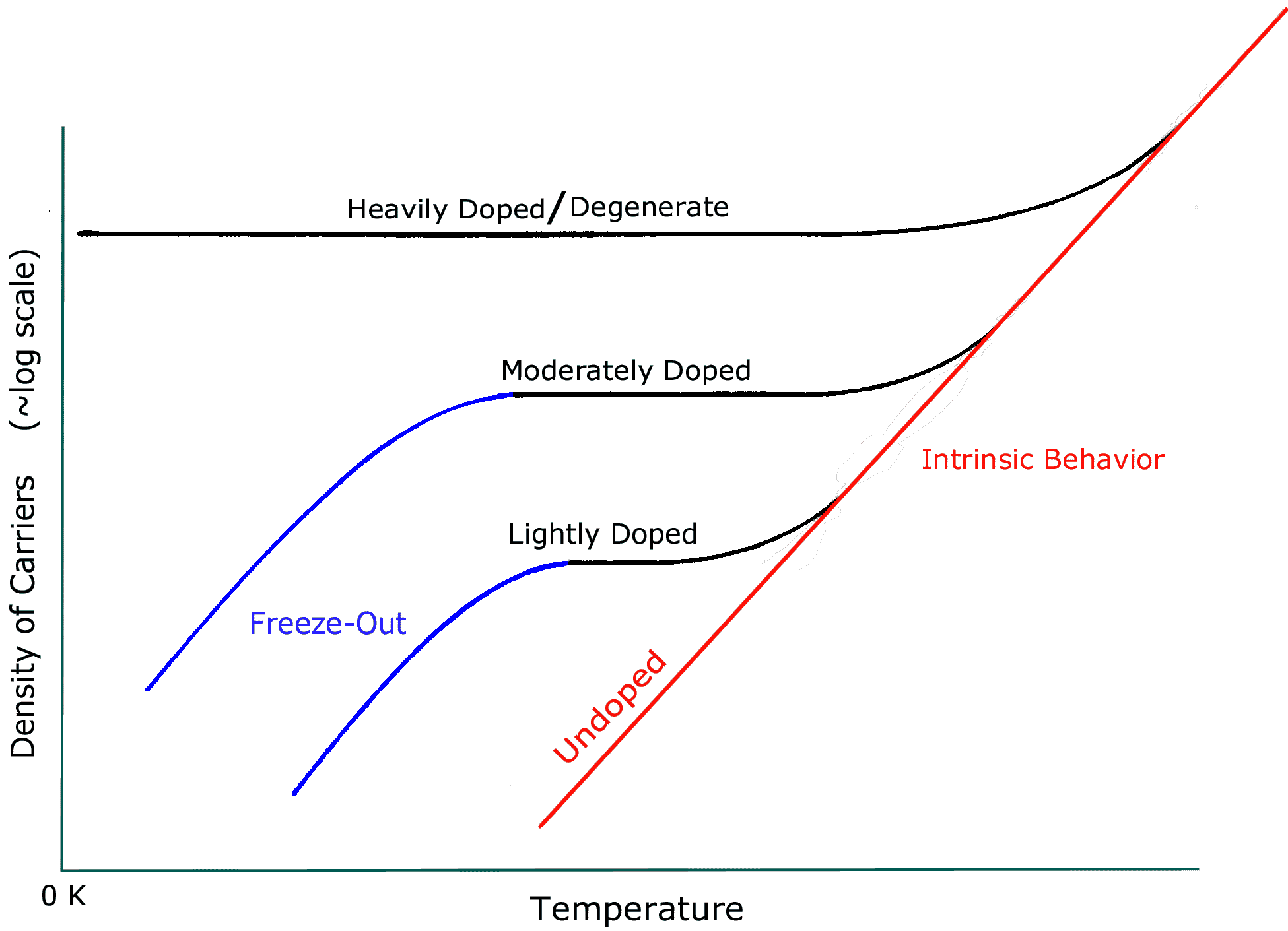
On the low-temperature end, there are additional effects that allow devices to operate below their "freeze-out" temperature. First, if the semiconductor is doped to a certain concentration, it can attain degeneracy, a condition in which the dopants require no energy for ionization. For example, this happens in n-GaAs at a fairly low doping concentration (~1016 cm-3) that is common in standard devices. Thus, standard GaAs MESFETs can operate down to the lowest temperatures, essentially to absolute zero. For Si, degenerate doping requires a much higher a concentration (~1019 cm-3). On the other hand, there are effects that prevent operation even before the device is cooled to the "freeze-out" temperature. For example, standard Si bipolar transistors cease operating well above the Si "freeze-out" temperature, as described later.
15) How do temperature capabilities differ between the two main types of devices: field-effect transistors and
bipolar transistors?
Low temperature
Field-effect transistors (FETs): Characteristics of FETs generally improve with cooling, such astransconductance, leakages, and white (high-frequency) noise (although Si JFETs degrade below about 100 K); low-frequency noise is less predictable.
The low-temperature limit of field-effect devices depends on the particular type and material: Si JFETs, are limited by their freeze-out temperature (about 40 K), but their performance actually degrades at a higher temperature. Ge JFETs have a similar behavior, although the relevant temperatures are lower, and under proper biasing can operate to the lowest cryogenic temperatures. Properly designed n-channel GaAs JFETs can also operate to the lowest temperatures, although they are uncommon.
Si MOSFETs, enhancement type, can also operate to the lowest temperatures because the carriers needed for conduction in the channel can be ionized by an electric field from the gate. Si MOSFETs and CMOS circuits are often used at deep cryogenic temperatures, below the freeze-out of Si.
Various types of heterostructure FETs (HEMTs or MODFETs), usually based on III-V semiconductors, do not require thermal energy to ionize the dopants. As a result, they can also be used over the entire cryogenic temperature range down to the lowest temperatures.
Bipolar transistors: Ordinary Si bipolars (Si BJTs) suffer a rapid decline in gain with cooling and are unusable below about 100 K. This in not a result of "freeze-out" but of low emitter-base injection efficiency. This effect can be avoided by adjusting the band gaps through "bandgap engineering" as in heterojunction bipolar transistors (HBTs), such as those based on SiGe. HBTs have demonstrated operation down to very low cryogenic temperatures and show increased performance on cooling. On the other hand, conventional homojunction Ge and GaAs bipolar transistors have also been reported to operate to very low cryogenic temperatures.
High temperature
Both field-effect and bipolar transistors can operate to high temperatures. The demonstrated temperature capability of field-effect and bipolar transistors has been similar for most semiconductor materials investigated. For BJTs and MOSFETs based on Si, operation has been reported to about 450°C and 500°C, respectively.
Performance of field-effect transistors typically declines steadily with increasing temperature, whereas the performance of bipolars (Si) shows an increase up to a point and then declines. For both field-effect and bipolar transistors the major cause of declining performance as temperature increases is increasing leakage in the p-n junctions. In MOS transistors these are the isolation junctions between source or drain and the body, in bipolar transistors it is the junctions that make up the transistor, especially the collector-base junction.
16) How does device design affect temperature capability?
As mentioned, for high temperatures, a primary limitation is leakage in the p-n junctions of a device.
As temperature rises this becomes excessive, rendering the device inoperative.
However, leakage can be reduced by several means, one of which is to reduce the area of the p-n junctions (or to eliminate them).
This can be done by scaling down device dimensions, or a very effective means for MOS transistors is to use silicon-on-insulator
(SOI) wafers. In these wafers the "bottom" of a MOSFET is a buried insulating layer of SiO2, rather than the
bulk semiconductor, and the "bottoms" of the p-n source and drain junctions are thus absent. This has allowed considerable
extension of the high-temperature limit for MOSFETs, by about 50−100°C. SOI provides other benefits such as inhibiting latch-up.
For low temperatures, the device design is less important than the other factors above in 14 and 15. The primary concerns are freeze-out
and its effects. For example, it is important to have sufficient doping concentration in the contact regions to avoid freeze-out
(appropriate to the particular semiconductor material and dopant type). Although Si MOSFETs can be used to the lowest temperatures,
certain design features are needed if anomalies, such as the "kink" effect and hysteresis, are to be minimized at deep
cryogenic temperatures (below Si freeze-out at approximately 40 K). These and other effects arise from charge trapping, which
becomes increasingly troublesome as temperature decreases. Operating bipolar transistors at cryogenic temperatures always requires
special designs and/or materials, a prevalent approach being the use of heterostructures as mentioned earlier.
The preceding has been adapted from the Extreme-Temperature Electronics Newsletter Issue #3 (5 October 2001).
Please keep in mind that the above material is only a general overview; the coverage is abbreviated and many points are only touched on.
Further information may be obtained from the included Internet link and from the items listed separately.
Return to top of page
¦ Part 1
¦ Part 2
¦ Part 4
Home
Most recent update: 23 November 2021
Copyright © 2001, 2003, 2021 by Randall K. Kirschman. All rights reserved.
